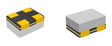
Wafer level Pad electrode processes for Surface Mount Devices
Some Si base devices can only packaged by wire bond processes, because they had insufficient substrate isolation characteristic.
AFSC had developed a "wafer level chip sidewall isolation technology", which can form an isolation barrier on chip sidewall to prevent solder short to Si substrate while SMT process.
This wafer level chip sidewall isolation technology can change the wire bond devices to SMD type devices, which has smaller package area and cheaper package coat.